

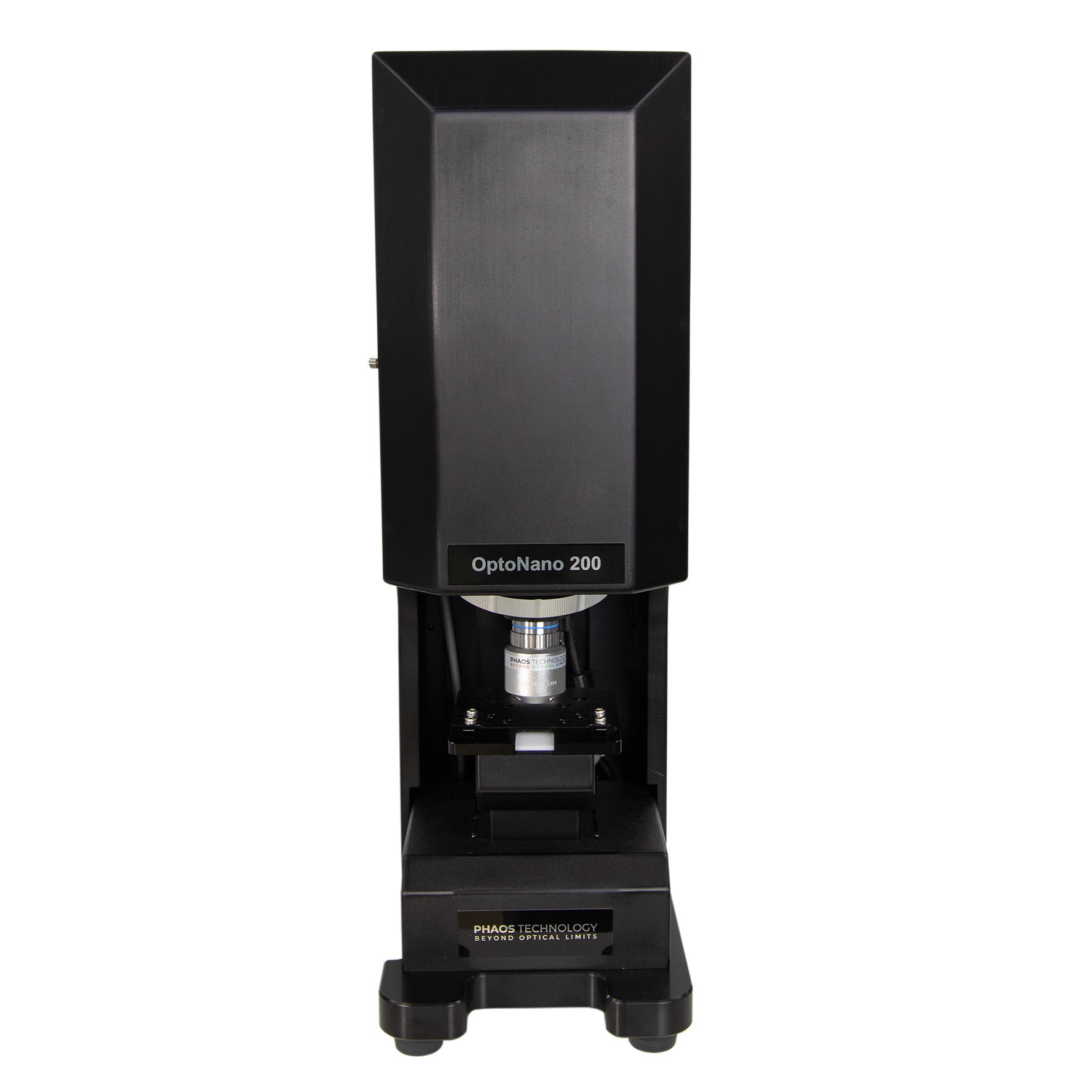
Key Features
- Interference Lens
- Air-Bearing Isolation System
- Sonic Vibration Isolation
- Easy level
- Convenient Joystick
- Vacuum Object Table
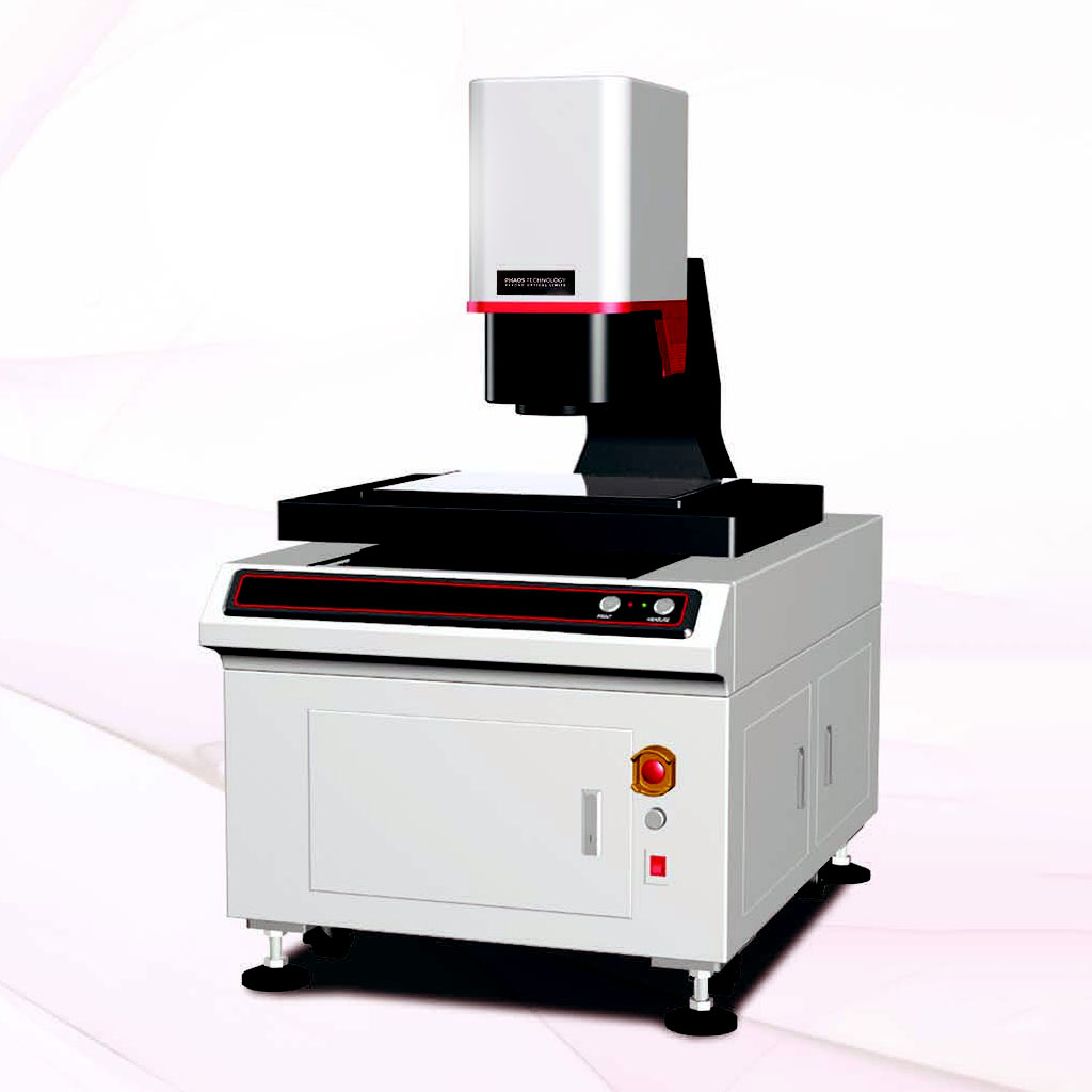
Dedicated Functions for Semiconductor Field
- Measure profiles trenches after laser grooving in the dicing process
- Measure film step-height of wafer ranging from 1nm~1mm.
- Measure roughness of silicon cut sheet after grinding process, and can measure dozens of small areas to obtain the average value by one click.
- Support 6″, 8″ and 12″ wafer measurement, and easy switch between 3 sizes of vacuum chucks by one click automatically.
Application
- It is used for measurement and analysis of surface roughness and profile of precision components from industries of semi-conductor, 3C Electronics, ultraprecise machining, optical machining, micro-nano materials, micro-electro-mechanical system
- Measurement and analysis for various products, components and materials’ surface form and profile characteristics, such as flatness, roughness, waviness, appearance, surface defect, abrasion, corrosion, gap, hole, stage, curvature, deformation, etc.
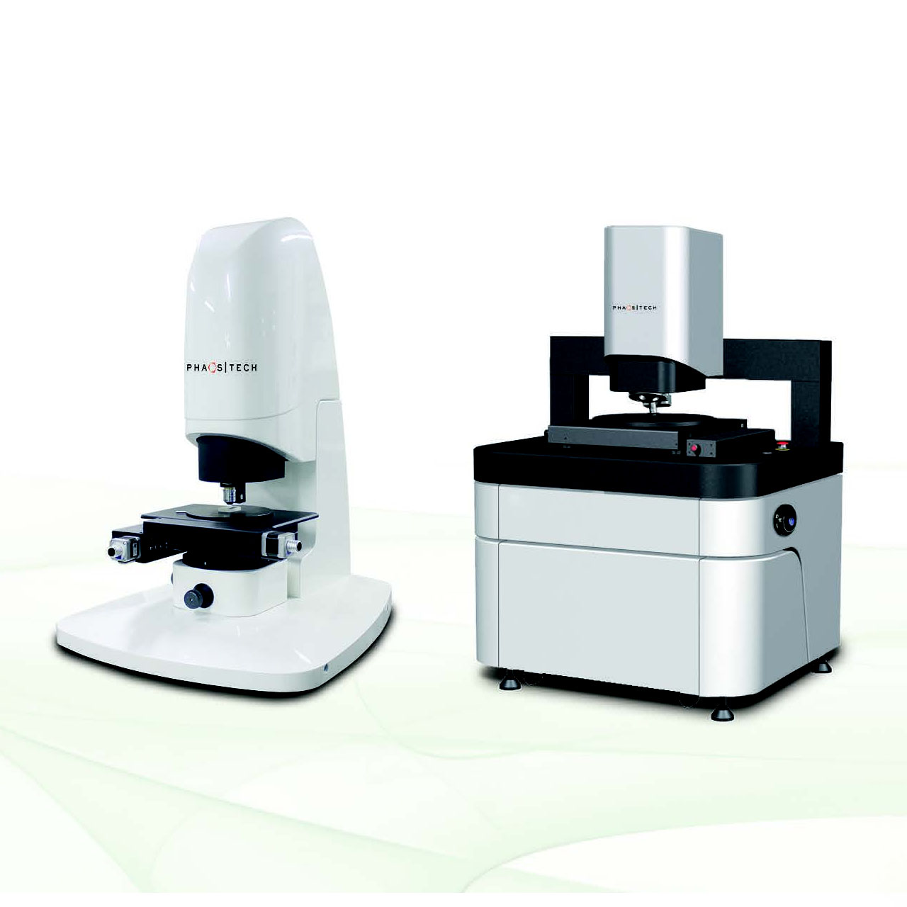
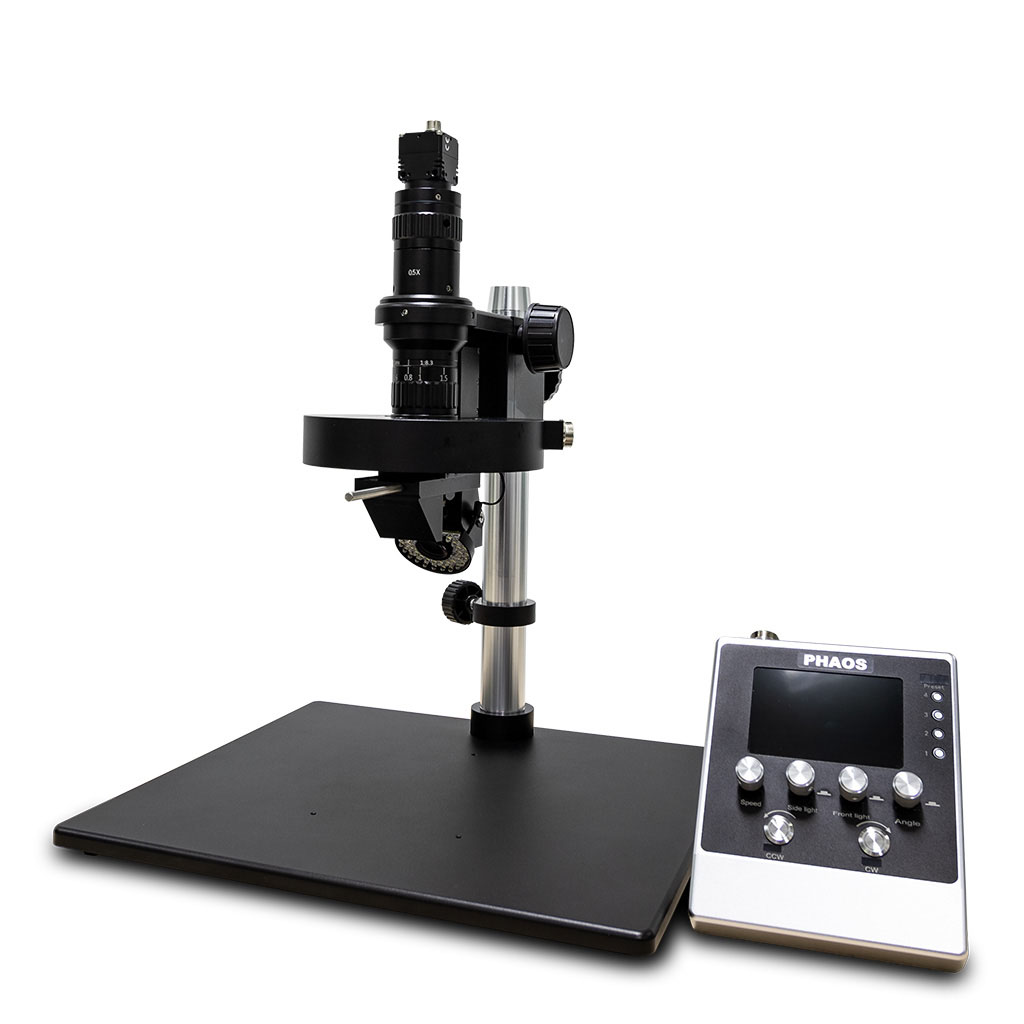
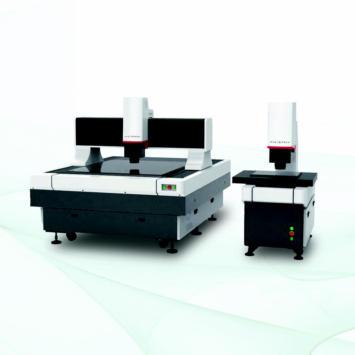
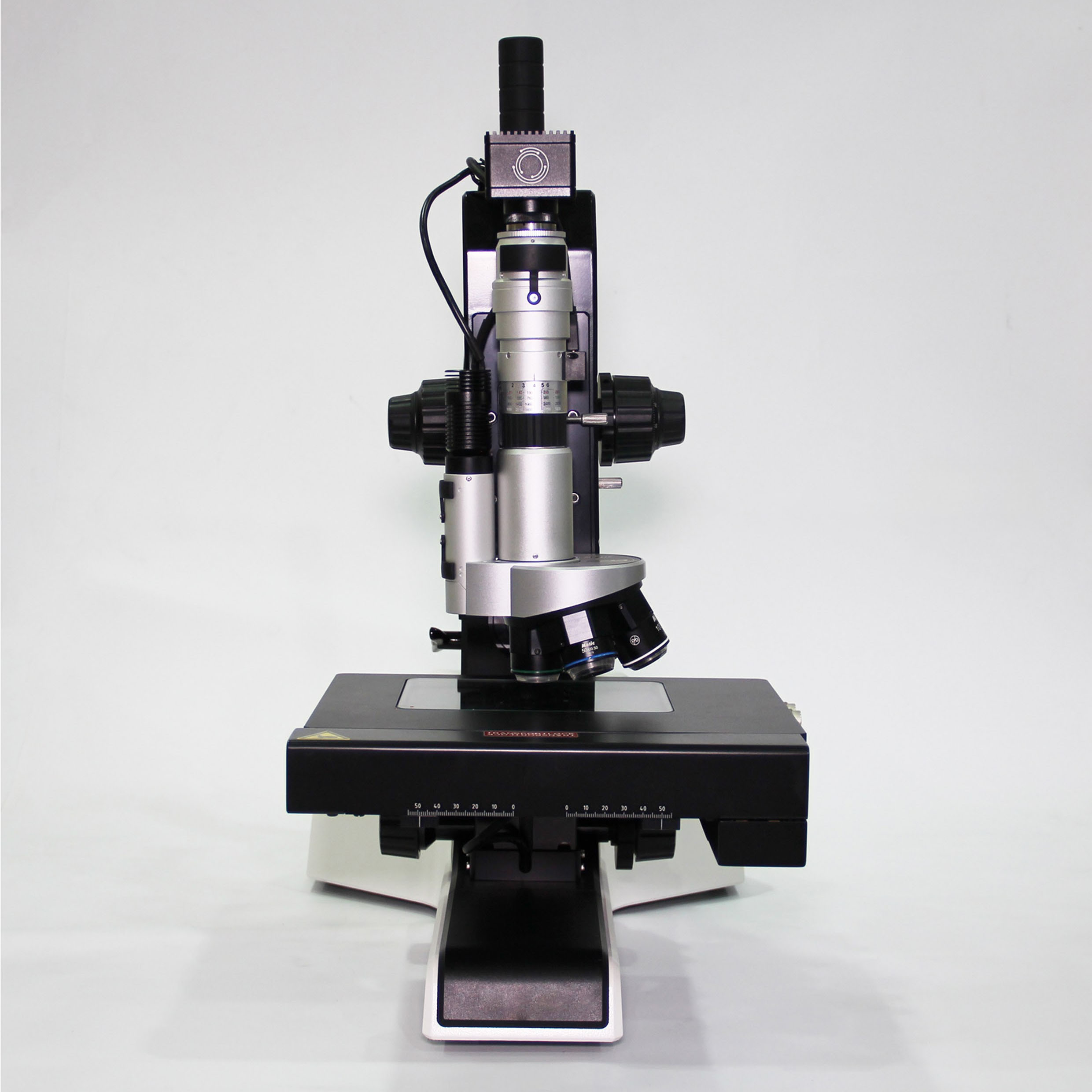
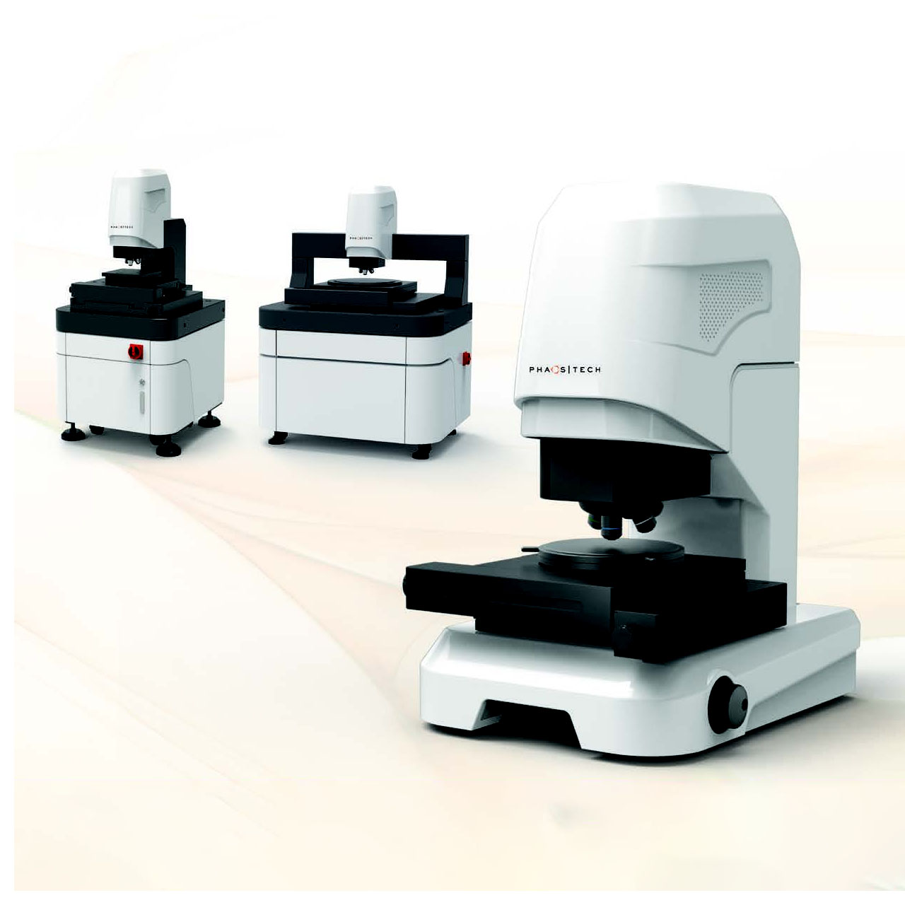
Related products
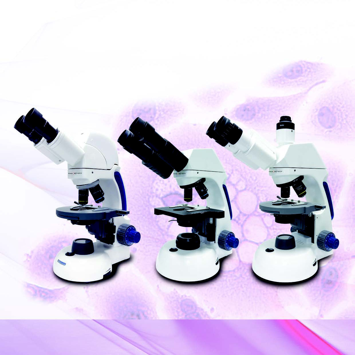
Optical Microscope
Optical Microscope
Optical Microscope
Optical Microscope
Optical Microscope
Optical Microscope
Optical Microscope
Optical Microscope